Basic Calculation of a Buck Converter’s Power Stage
Abstract
This application note gives the formulas needed to design the power stage of a buck converter. Switched mode power converters are very important in industry. The synchronous buck converter is used to step a voltage down from a higher level to a lower level. This application note describes how to determine the buck inductor and input and output capacitors. Good design can improve performance and help to meet customer requirements. Because of this, it is important to understand the fundamentals of the synchronous buck converter and how to appropriately select the circuit components.
Synchronous Buck Converter Basics
The synchronous buck converter is used to step a voltage down from a higher voltage to a lower voltage. Synchronous buck converters are very popular in industry today and provide high efficiency solutions for a wide range of applications. This application note gives the formulas to calculate the power stage of a synchronous buck operating in continuous conduction mode.
A synchronous buck converter produces a regulated voltage that is lower than its input voltage and can deliver high current while minimizing power loss. As shown in Figure 1, the synchronous buck converter is comprised of two power MOSFETs, an output inductor, and input and output capacitors.
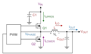
Figure 1. Basics of a synchronous Buck converter.
Q1, the high side MOSFET, is connected directly to the input voltage of the circuit. When Q1 turns on, IUPPER is supplied to the load through Q1. During this time the current through the inductor increases (charging L) and Q2 is off. When Q1 turns off, Q2 turns on and ILOWER is supplied to the load through Q2. During this time, the inductor current decreases (discharging L). Figure 2 shows the basic waveforms for the synchronous buck converter in continuous conduction mode.
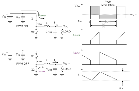
Figure 2. Synchronous buck converter waveforms
Calculate the Inductor Current
There are conduction losses in components that are important in determining D, the duty factor. Most important of these are the on resistances of the high- and low-side MOSFETS (Q1 and Q2). Taking these losses into account, we can now express the duty cycle of the buck converter as:
where VDSQ1 is the voltage differential across the high-side MOSFET and VDSQ2 is the voltage differential across the low-side MOSFET. The next step is to determine the inductor ripple current.
Inductor Ripple Current : 
where VIN is the input voltage, VOUT is the output voltage, fS is the switching frequency of converter, and L is the selected inductor value.
The peak inductor current is the average current pulse half the inductor ripple current.
Maximum inductor current : 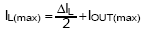 ,
,
where IOUT(max) is the maximum output current and IL(max) is the peak inductor current. The IC’s current limit must exceed IL(max). Putting it another way, the highest reliable output current from a particular IC depends on the minimum value of its current limit.
Maximum output current of the selected IC : 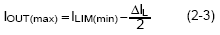
where ILIM(min) is the minimum value of the IC’s current limit.
Basic Inductor Design
The output of the synchronous buck converter consists of an inductor and capacitor. The output stage stores and delivers energy to the load and produces a constant output voltage. Inductors are manufactured in various materials and with a wide range of values, typically having a tolerance of ±20%. Inductors have an inherent DC resistance (DCR) which impacts the performance of the output stage. Minimizing the DCR (with all other parameters held constant) improves the overall efficiency of the converter.
There is a trade-off between inductance and ripple current: the lower the inductance, the higher the ripple current through the inductor. A minimum inductance must be met in order to guarantee a maximum ripple current and therefore, a maximum peak switch and inductor current.
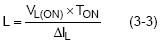
Calculating Minimum Inductance: Inductor current ripple is defined as the peak to peak change in current during the on and off time. For the synchronous buck converter, the change in inductor current during the high side MOSFET Q1 on time is equal to the change during the MOSFET’s off time. The inductor current increase is equal to the inductor current decrease.
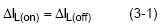
For the above reason, the inductor current ripple can simply be defined as ΔIL. We can calculate ΔIL beginning with the basic equation of inductance.
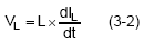
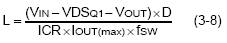
Where dIL = ΔIL, dt = TON, the on time of high side MOSFET. Solving for L and using the voltage across the inductor during the on time,
The voltage applied to the inductor during the on time is :
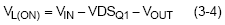
where VDSQ1 is the voltage drop across the high side MOSFET while it is on.
The duty cycle is defined as the ratio of high side MOSFET Q1 on time to the switching period of the converter.
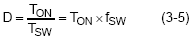
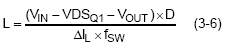
Using this fact, equation (3-3) becomes :
The ripple current ΔIL can also be expressed as the ratio of inductor current to full output current, or inductor current ripple ratio (ICR) :
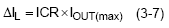
Substituting Equation (3-7) into Equation (3-6), the inductance becomes :
Equation (3-1) can be used to calculate the duty cycle, beginning with the inductor ripple during the on time and off time and using equation (3-5) :
Adding the fact that the voltage across the inductor during the off time is :
where VDSQ2 is the voltage drop across the low side MOSFET Q2 while it is on, setting  , and substituting Equations 3-9, 3-10, and 3-11, the duty cycle becomes :
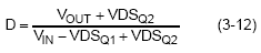
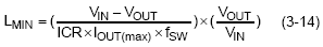
Therefore, the final inductance equation, LMIN, becomes :
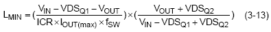
Equation (3-13) can be simplified by neglecting the VDSQ1 and VDSQ2, then the minimum inductance becomes
There is a tradeoff between inductance and ripple current. To optimize the output inductance, it is recommended to target an ICR of 20%-40% of IOUT(max).
Basic Output Capacitor Design
The output capacitor COUT maintains the regulated output voltage during the times when the inductor current is higher or lower than the output current. This occurs each cycle as the inductor current ripples up and down, and during output load changes before the inductor current reaches the required new average level. The amplitude of the capacitive sag is a function of the load step, the output capacitor value, the inductor value, the input-to-output voltage differential, and the maximum duty cycle. which is as fast as allowed. Calculate the approximate on-time
(neglect parasitics) and maximum duty cycle for a given input and output voltage as :
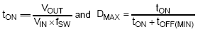
The actual on-time will be slightly longer as the IC compensates for voltage drops in the circuit, but we can neglect both of these since the on-time increase compensates for the voltage losses. Calculate the output voltage sag as:
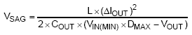
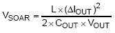
The amplitude of the capacitive soar is a function of the load step, the output capacitor value, the inductor value and the output voltage :
The output voltage ripple, , is defined as the peak to peak fSW ripple voltage superimposed onto the DC output voltage. The capacitor voltage ripple can be expressed as a ratio of the ripple to the total output voltage, CVRR.
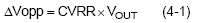
where CVRR = ΔV / VOUT
Usually CVRR is limited to less than 1~2% of the output voltage.
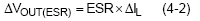
The equivalent series resistance (ESR) of COUT influences the response time of regulator’s feedback loop and is also one component of the output voltage ripple :
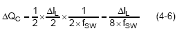
Each cycle, when the inductor current exceeds the output current, the output capacitor voltage increases. When the inductor current is less than the output current, the output capacitor voltage decreases. To achieve the correct average output current and a constant DC output voltage, the amount of the output capacitor charging must be equal to the amount of output capacitor discharging. The steady avenge state current through the capacitor is 0A (Figure 3.)
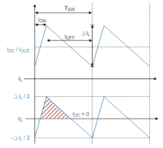
Figure 3. Inductor and capacitor current
The current through the COUT is defined as:
(4-3) can be written as :
The red shaded area in Figure 3 shows the area under the inductor current curve, equal to the COUT charge energy :
:
where 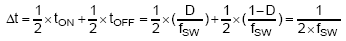
Since , equation (4-5) can be written:
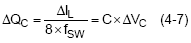
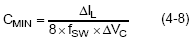
The minimum output capacitance depending on the output capacitive ripple voltage, can be determine by (4-7)
The total output voltage ripple consists of the ESR ripple (4-2) and the capacitive ripple (4-7). To meet a specific maximum ripple requirement you could allow half of the specification for each component of the ripple. Typically, one ripple component dominates and should be allotted more than half of the ripple allowance. For MLCC output capacitors, the capacitive ripple is the greater portion, while for electrolytic or tantalum capacitors, the ESR typically dominates.
Input Capacitor Selection
The buck’s input current is discontinuous, turning on when S1 is on and off when S1 is off. Since the input voltage source (battery, AC/DC adapter, etc.) is typically unable to support the required rapid current changes, the input capacitor supplies this changing current to S1 and the inductor. By supplying the required changing current, the capacitor holds the input voltage fairly steady. The input capacitor is discharged slightly during S1’s on time and recharges during the off time.
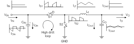
Figure 4.Buck converter Power Stage
The changing current and constant charging and discharging creates heat in the input capacitor that can degrade its lifetime or even quickly destroy it. The input ripple current (IRMS) can be expressed as:
Usually the manufacturer's maximum capacitor ripple current (called Ripple Current), refers to the actual current flowing through the capacitor. This RMS current passing through the capacitor’s ESR will produce Joule loss, causing the temperature to rise; the formula is . Manufacturers specify a maximum ripple current to limit the temperature rise. Because most ceramic capacitors have very low ESR (about 5mΩ), there is less need to worry about excessive ripple current specifications.
The input capacitor (or group of input capacitors) must be able to handle the required IRMS. Some capacitors have RMS current ratings but many do not. Therefore, it may be useful evaluate the capacitor voltage ripple instead. From the basic capacitor equation:
Neglecting power losses, the average DC input current is given by

It is assumed that the DC component of input current is provided by the input voltage source and the AC component by the input filter capacitor. Neglecting inductor ripple current, the input capacitor sources current of amplitude IO-IIN during the D interval as S1 conducts. Conversely, the capacitor is charged by IIN during the 1-D interval when S2 conducts. With the current polarity as indicated, this can be written as
where Ts is the switching period. Thus, the input capacitor conducts a square-wave current of peak-to-peak amplitude Io and it follows that the resultant capacitive component of AC ripple voltage is a triangular waveform with peak-to-peak amplitude specified by equation (5-1).
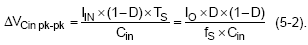
The maximum ripple voltage occurs at 50% duty cycle (5-4).
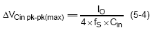
As a general rule of thumb, keep the peak to peak ripple amplitude below 75mV.
Output Voltage Setting
Figure 6 show Buck converters sense the output voltage with a resistive divider network. With a given feedback voltage, VFB, the voltage divider can be calculated.
The current through the resistive divider is recommended to be at least 100 times larger than feedback bias current: IR1/2 ≤ 100 x IFB, (6-1)
Where IFB is the feedback bias current from the IC datasheet and IR1/2 is the current through the feedback divider.
The divider current can be a lot higher, which may increase output voltage accuracy due to reduced noise coupling. The only disadvantage of smaller resistor values is a higher power loss in the resistive divider.
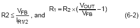
where VFB is the feedback voltage from the datasheet and VOUT is the desired output voltage.
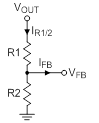
Figure 6. Resistice divider for setting the output voltage
Summary
In synchronous buck converters, careful selection of inductors and input and output capacitors is necessary to get better performance and to meet customer requirements. This application note performed detailed analysis and design to select suitable inductance and input and output Capacitance